- 您现在的位置:买卖IC网 > Sheet目录362799 > EVAL-AD1837EB (Analog Devices, Inc.) 2 ADC, 8 DAC, 96 kHz, 24-Bit Codec
REV. B
AD1837
–7–
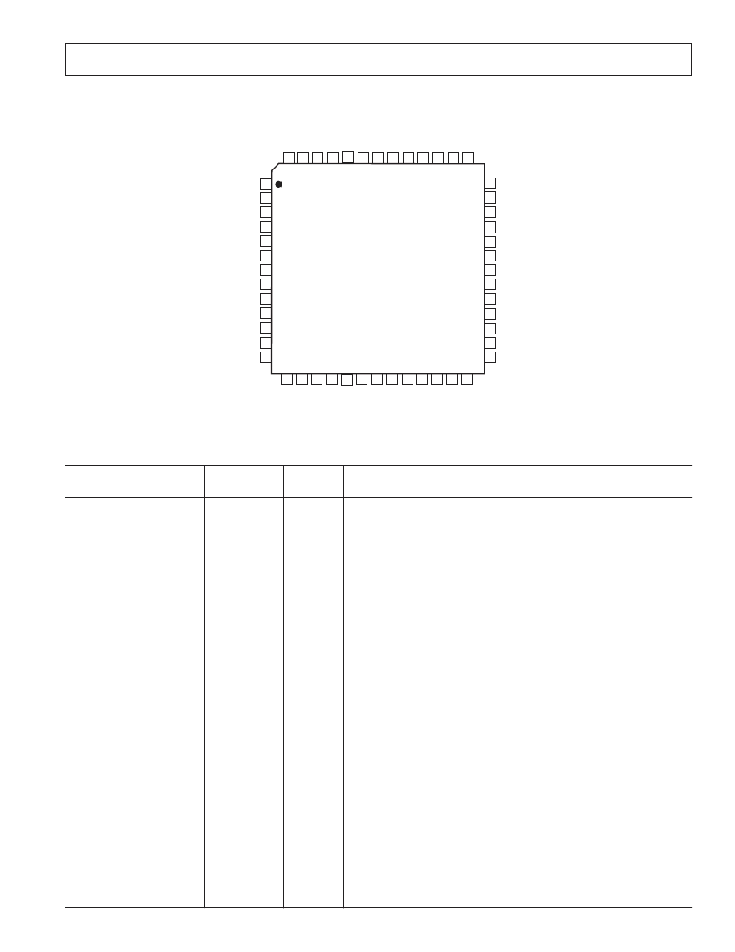
PIN CONFIGURATION
1
2
3
4
5
6
7
8
9
10
11
12
13
A
AVDD
O
N
OUTL2
NC
OUTR1
NC
OUTL1
NC
PD
/
RST
CIN
CLATCH
DVDD
N
O
NC
OUTR3
NC
OUTL4
NC
OUTR4
AGND
DLRCLK
DBCLK
D
14
15
16
17
18
19
20
21
22
23
24
25
26
27
28
29
30
31
32
33
34
35
36
37
38
39
52
51
50
49
48
47
46
45
44
43
42
41
40
F
F
AGND
M
/S
AGND
A
A
A
A
A
A
AGND
D
C
C
A
O
M
A
A
D
D
D
D
DVDD
AVDD
AD1837
TOP VIEW
(Not to Scale)
NC NO CONNECT
PIN FUNCTION DESCRIPTIONS
Input/
Output
Pin No.
Mnemonic
Description
1, 39
2
3
4
5, 10, 16, 24, 30, 35
6, 8, 12, 14, 25, 27, 31, 33
7, 13, 26, 32
9, 15, 28, 34
11, 19, 29
17
18
20
21
22
23
36
37
38
40, 52
41–44
45
46
47
48
49
50
51
DVDD
CLATCH
CIN
PD
/
RST
AGND
NC
OUTLx
OUTRx
AVDD
FILTD
FILTR
ADCLN
ADCLP
ADCRN
ADCRP
M
/S
DLRCLK
DBCLK
DGND
DSDATAx
ABCLK
ALRCLK
MCLK
ODVDD
ASDATA
COUT
CCLK
Digital Power Supply. Connect to digital 5 V supply.
Latch Input for Control Data.
Serial Control Input.
Power-Down/Reset.
Analog Ground.
Not Connected.
DACx Left Channel Output.
DACx Right Channel Output.
Analog Power Supply. Connect to analog 5 V supply.
Filter Capacitor Connection. Recommended 10
m
F/100 nF.
Reference Filter Capacitor Connection. Recommended 10
m
F/100 nF.
ADC Left Channel Negative Input.
ADC Left Channel Positive Input.
ADC Right Channel Negative Input.
ADC Right Channel Positive Input.
ADC
Master
/Slave Select.
DAC LR Clock.
DAC Bit Clock.
Digital Ground.
DACx Input Data (Left and Right Channels).
ADC Bit Clock.
ADC LR Clock.
Master Clock Input.
Digital Output Driver Power Supply.
ADC Serial Data Output.
Output for Control Data.
Control Clock Input for Control Data.
I
I
I
O
O
I
I
I
I
I
I/O
I/O
I
I/O
I/O
I
O
O
I
发布紧急采购,3分钟左右您将得到回复。
相关PDF资料
EVAL-AD1837AEB
2 ADC, 8 DAC, 96 kHz, 24-Bit Codec
EVAL-AD1838AEB
2 ADC, 6 DAC, 96KHZ 24 BIT CODEC
EVAL-AD1852EB
24-Bit Stereo DAC Evaluation Board
EVAL-AD1870EB
Single-Supply 16-Bit Stereo ADC
EVAL-AD1896EB
Automotive Low-Cost Non-Volatile FPGA Family; Voltage: 1.2V; Grade: -5; Package: Lead-Free ftBGA; Pins: 256; Temperature: AUTO; LUTs (k): 8
EVAL-AD1928EBZ
2 ADC/8 DAC with PLL, 192 kHz, 24-Bit Codec
EVAL-AD1928EB
2 ADC/8 DAC with PLL, 192 kHz, 24-Bit Codec
EVAL-AD1938EB
4 ADC/8 DAC with PLL, 192 kHz, 24 Bit CODEC
相关代理商/技术参数
EVAL-AD1838AEB
制造商:Analog Devices 功能描述:EVALUATION BOARD I.C. - Bulk
EVAL-AD1838EB
制造商:Analog Devices 功能描述:Evaluation Board For 2 ADC, 8DAC 96 KHz, 24-Bit Sigma Delta Codec 制造商:Analog Devices 功能描述:EVALUATION BOARD I.C. - Bulk
EVAL-AD1839AEB
制造商:Analog Devices 功能描述:EVALUATION BOARD I.C. - Bulk
EVAL-AD1839EB
制造商:Analog Devices 功能描述:EVALUATION BOARD I.C. - Bulk
EVAL-AD1852EB
制造商:Analog Devices 功能描述:Evaluation Kit For 24Bit Stereo DAC Evaluation Board 制造商:Analog Devices 功能描述:STEREO,192KHZ VLTG OUTPUT SGMA DELTA DAC - Bulk
EVAL-AD1852EBZ
制造商:AD 制造商全称:Analog Devices 功能描述:Stereo, 24-Bit, 192 kHz, Multibit, Sigma-Delta DAC
EVAL-AD1853EB
制造商:Analog Devices 功能描述:EVALBRD 192KHZ MULTIBIT SIGMA DELTA DAC - Bulk
EVAL-AD1854EB
制造商:Analog Devices 功能描述:Evaluation Board For AD1854 Stereo, 96 KHZ, Multibit Segma-Delta DAC 制造商:Analog Devices 功能描述:EVALBOARD 96KHZ MULTIBIT SIGMA DELTA DAC - Bulk